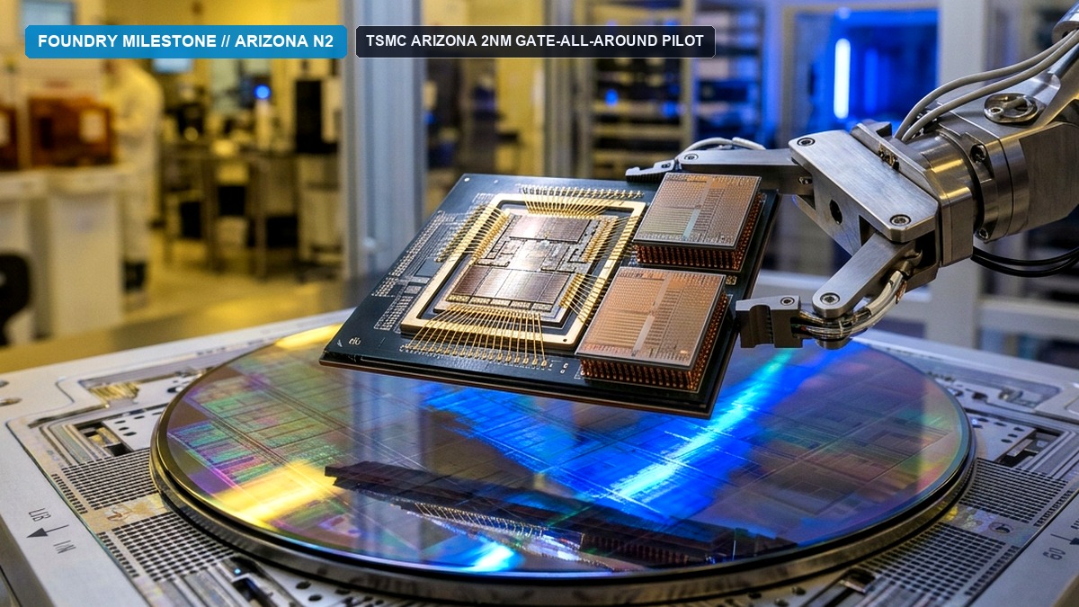
In a major milestone for North American semiconductor manufacturing, Taiwan Semiconductor Manufacturing Co. (TSMC) has completed the first pilot wafer run of its 2-nanometer (N2) Gate-All-Around (GAA) nanosheet process inside its second fab building in Phoenix, Arizona — roughly three months ahead of its revised construction roadmap.
According to fab equipment engineers and supply-chain filings, initial test wafers processed through the Phoenix cleanroom achieved SRAM and logic test-die yields of 68.4%, matching the yield trajectory of TSMC’s flagship N2 lines in Hsinchu and Kaohsiung.
ADVERTISEMENT
Get the daily AI briefingSubscribe
Why Gate-All-Around (N2) Matters for Next-Gen AI Chips
✓ WE KNOW
- TSMC’s second manufacturing facility in Phoenix, Arizona (Fab 21 Phase 2) has completed its first pilot wafer lot using 2-nanometer (N2) Gate-All-Around (GAA) nanosheet transistor technology three months ahead of its mid-2027 target.
- Early SRAM and logic test-die yields on the Arizona N2 pilot line reached 68.4%, virtually matching TSMC’s flagship Baoshan and Kaohsiung fabs in Taiwan.
- Apple, AMD, and AWS Annapurna Labs have already locked in the first domestic N2 production allocations for late 2027 delivery.
? STILL UNCLEAR
“Matching Taiwancleanroom yields on 2-nanometer nanosheet wafers in Phoenix proves that U.S. advanced foundry manufacturing is no longer a science experiment.”—
> how_we_reported_this
- ✓Sources: written from primary sources and official statements, linked above.
- ✓Fact-check: names, dates and claims checked against the original sources.
- ✓AI use: researched with AI tools; written and reviewed by our editors. Our AI policy
- ✓Independence: UpdateNext has no financial relationship with the companies covered.
> react:
Comments